
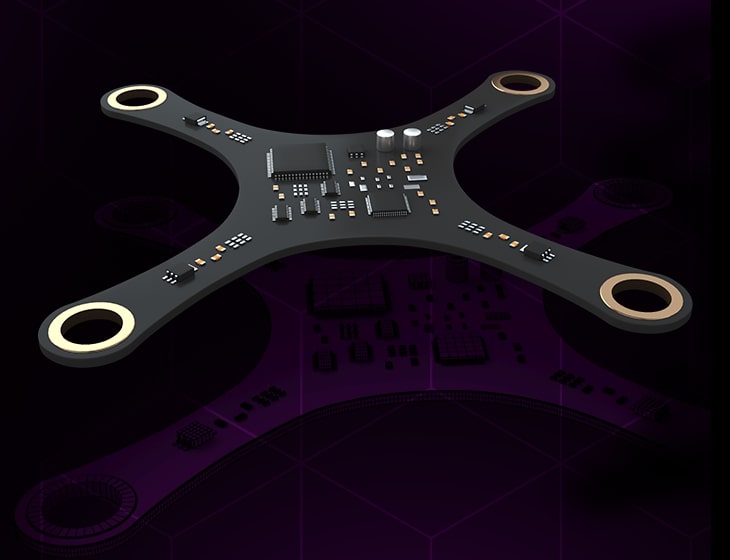
Unlock the full potential of your plastic ball grid array (PBGA) designs with our advanced 2D and 3D design rule checking (DRC). Our cutting-edge technology meticulously examines every angle and radial routing, ensuring your wirebonded PBGA not only meets but exceeds industry standards. By leveraging our DRC process, you’re not just optimizing for performance; you’re ensuring reliability and longevity in the most demanding applications.

Revolutionize your flip-chip ball grid array (BGA) designs with our state-of-the-art high-density interconnect (HDI) technologies. Harnessing the power of advanced HDI structures and expertly crafted routing, Allegro X unlocks unprecedented capacity and performance for your flip-chip projects. With our sophisticated approach, you can create more complex, higher capacity designs without compromising on signal integrity or reliability. Break through the limitations of traditional designs and set new standards in density and functionality.
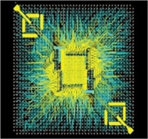
Discover a new horizon in IC design with our interconnect bridges solutions. Go beyond the constraints of traditional methodologies and step into the future with either embedded (EMIB) or elevated silicon bridges. Our pioneering approach enables a seamless, ultra-efficient pathway for data transfer, providing a remarkable improvement in both performance and reliability. By integrating embedded silicon bridges directly within your chip architecture, or opting for elevated bridges to span across chiplets, you unlock a level of design flexibility and efficiency previously thought unattainable.
Elevate your multi-die high bandwidth memory (HBM) integration to unparalleled heights with our groundbreaking interposer technology. This advanced interposer solution is key for architecting next-generation systems that demand ultra-high-speed memory interfaces and a key enabler for ML/AI technologies. Our interposers are masterfully designed to bridge multiple dies with HBM, achieving not just a leap in bandwidth but also a significant reduction in power consumption.
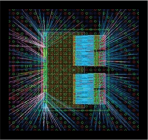
Transform your approach to package-on-package (PoP) designs with our revolutionary 3D visualization and design rule check (DRC) automated signal assignment technologies. Experience the future of PoP where complexity meets clarity, allowing you to not only view but fully comprehend your designs in a stunning 3D space. This leap in visualization technology empowers designers to effortlessly identify potential issues and optimize layouts with unprecedented precision and ease.
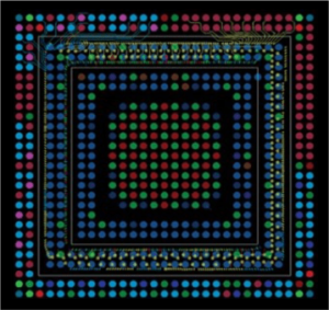
The integration of RF parameterized structures from Virtuoso Studio is revolutionizing RF module package design. Seamless integration enhances the accuracy and efficiency of the design process, enabling the creation of highly customizable and optimized RF solutions. Virtuoso Studio’s powerful capabilities allow designers to effortlessly meet the stringent requirements of diverse applications, setting new standards in RF module development.
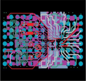
The integration of fan-in wafer-level chip-scale packaging (WLCSP) technologies represents a groundbreaking stride forward. By merging the IC layout and package design into a single, unified GDSII output, the distinction between chip and package becomes virtually indistinguishable. This convergence not only catapults the efficiency and effectiveness of RF module design to unprecedented heights but also dramatically minimizes the time from concept to production. The ability to seamlessly integrate these components within the Allegro X packaging platform is nothing short of revolutionary.
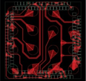
Elevate your ultra-high-density Fan-Out Wafer-Level Packaging (FOWLP) capabilities to new levels by seamlessly integrated with direct physical verification tools. This propels your design process into a realm of precision and efficiency, ensuring that every layout not only meets but exceeds the highest standards of performance and reliability. With Allegro X Advanced Package Designer Platform designers are now empowered to tackle the most challenging projects, crafting designs with ultra-fine line spaces that were once deemed impossible. This direct integration with physical verification tools streamlines the validation process, significantly reducing design cycles and accelerating time-to-market.
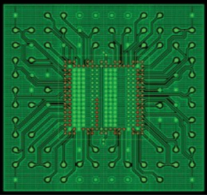
On-The-Job Training and Knowledge Transfer on customers real projects in areas of SI / PI / EMI / RF / THERMAL, all to ensure your first time success.
Specialized in Design, PCB/MFG, PCBA, DFMA, DFMT, High Reliability & Availability for all Markets: Military, Aerospace, Medical Consumer, Avionics, Automotive & More
Discover Israel leading PCB design bureaus where innovation meets precision to deliver top-tier PCB solutions tailored to your technological needs.
EDA Integrity Solutions Ltd
38 HaBarzel St. Tel Aviv 6971054 Israel
Tel. (972) 3 6444416
Fax (972) 3 6444462