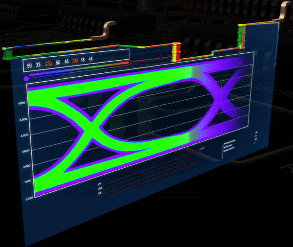
Cadence’s industry-leading distributed multiprocessing technology in the Clarity 3D Solver delivers the virtually unlimited capacity and 10X speed required to efficiently and effectively address larger and more complex structures. It creates highly accurate S-parameter models for use in high-speed signal integrity (SI), power integrity (PI), high-frequency RF/microwave applications, and electromagnetic compliance (EMC) analysis, enabling simulation results that match lab measurement, even at 112Gbps+ data transfer speeds.
The Clarity 3D Solver makes it easy to analyze systems, PCBs, packages, and other high-speed interfaces. Simulate complex geometries and structures to extract highly accurate S-parameter models for use in SI, PI and RF analysis.

Kristoffer Skytte, Cadence senior principal application engineer, presents a Clarity 3D Solver case study sharing the experience and best practices for achieving measurement-to-simulation correlation based on the Wild River CMP 50 IEEE P370 compliant test fixture where lab measurements were taken from DC to 50GHz. This presentation discusses topics such as material property identification, correlation challenges, influence of connector models, and manufacturing tolerance/variation.
Electromagnetic (EM) simulation of large chip-package designs using the Cadence Clarity 3D Solver is discussed by Nicholas Swart, principal CAD engineer at Analog Devices. Learn about detailed results of the Clarity simulation performance obtained on ADI’s compute farm, where the company easily simulated a large, complex system-on-chip (SoC) laminate in approximately 15 hours with modest per-machine memory consumption.
How to extract highly accurate S-parameter models for SI, PI and EMC analysis to ensure design reliability.
Check out how to simulate an edge-coupled filter using Cadence AWR Microwave Office software and Cadence Clarity 3D Solver.
On-The-Job Training and Knowledge Transfer on customers real projects in areas of SI / PI / EMI / RF / THERMAL, all to ensure your first time success.
Specialized in Design, PCB/MFG, PCBA, DFMA, DFMT, High Reliability & Availability for all Markets: Military, Aerospace, Medical Consumer, Avionics, Automotive & More
Discover Israel leading PCB design bureaus where innovation meets precision to deliver top-tier PCB solutions tailored to your technological needs.
EDA Integrity Solutions Ltd
38 HaBarzel St. Tel Aviv 6971054 Israel
Tel. (972) 3 6444416
Fax (972) 3 6444462